For discussion of Speeduino compatible boards designed / built by other members of the forum and for guidance around making such a board
User avatar
By Bleeker
#24066
To avoid any confusion I think it´s better to open another Thread for my version of NO2C.
Actually no overhang is wrong, as I had to stretch the PCB by arround 16mm to get everything placed on it.

Here is a short overview about my changes:

- added LM1815 VR conditioner
- removed on board MAP
- added input for external MAP
- placed TE Connectivity Ampseal connector with 23 Pins:
http://www.te.com/usa-en/product-770669-1.html

With this arrangment the traces require a lot of space, my current status is this:
NO2C+Ampseal PCB Header.JPG
NO2C+Ampseal PCB Header.JPG (285.31 KiB) Viewed 11295 times
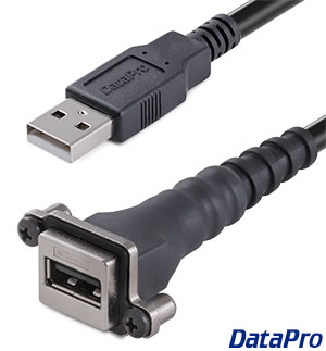
The USB Header and the DC Connector on the Mega will have to be desoldered, as they would clash with the Ampseal connector. The USB will be replaced with something like this:
Image

What is missing is the Stepper Header and the grounding, but before I finish this I have a few questions, which I guess are mostly adressed to Weaver :D

Question 1:
When I load the Net List I get a lot of Errors regarding Pins on Shield 1 which can not be found, is this normal?

If you find any other Issues, just let me know. I will also Post the schematic later, but first I have to find out how to rename the Project, as I have startet working on the original NO2C Project which I have downloaded :oops:

Also I have already Designed a enclosure, but my HDD crashed and I don´t know if I can recover the files :(
By dazq
#24068
Looking good!
One comment, stay under 100mm long dimension. PCB fab jumps hugely after 100mm
#24069
Looks like you are coming along nicely.
Bleeker wrote:With this arrangment the traces require a lot of space
I know, right! Definitely a factor in why the connector went in the center on the NO2C. Getting all the connections down to the other end can be a big pain.
Bleeker wrote:What is missing is the Stepper Header and the grounding
Did you remove the fills on the front and back?
Bleeker wrote:When I load the Net List I get a lot of Errors regarding Pins on Shield 1 which can not be found, is this normal?
Yes, this is because I deleted pins from the PCB so i could use some of that space, but left the pins in the schematic in case I wanted to bring them back. So don't use any of them that I removed unless you add them back. :)
Bleeker wrote:how to rename the Project
Rename the folder and all the file prefixes. The GERB, RENDER, DOC, and BOM folders I added in there and you can delete. Then open it and click the blank page with the arrow icon at the top to edit the information in the corner of the schematics and PCB prints.
Bleeker wrote:Also I have already Designed a enclosure, but my HDD crashed and I don´t know if I can recover the files
That's some bad luck there man! :(
User avatar
By Bleeker
#24086
dazq wrote:Looking good!
One comment, stay under 100mm long dimension. PCB fab jumps hugely after 100mm
Oh, I was not aware of that, I will definetly check the rates for my board before finishing it, but I guess reducing to 100mm will not be possible :(
turboedge wrote: I know, right! Definitely a factor in why the connector went in the center on the NO2C. Getting all the connections down to the other end can be a big pain.
The Ampseal Header is also available in a vertical version, this could stay in the middle of the board I guess.
turboedge wrote:
Bleeker wrote:What is missing is the Stepper Header and the grounding
Did you remove the fills on the front and back?
Yes, but I think kicad is creating them automaticly, right?
I have not tried the filling before, would it have been better if I had left them?

I also have a question regarfding the clamp protection, the SP721 only provides 6 connections, but I would actually need 2 more (for MAP and 2nd Tach). Should I just remove the 2 missing ADC Clamps on the Inputs which I will not use primary or is there a type which has 8 connections?

Regards, Björn
By dazq
#24087
Look on the little Fuse web site there is a 8 Ch version of the sp721 but is only in smd format iirc

Edit
Look on web site there is a sp720 it is a 16pin pdip or soic and has 14 channels of protection!!
#24093
Ceeloo Yello wrote:This should be called SO2C then (Some Overhang)
:lol: Perfect!

I believe you will have to increase the size of the planes, I don't think they will automatically grow with the edge cuts. If you are running the primary tach through a VR conditioner you probably won't need the clamp on that I would not think. You can definitely up-size to the SP720 (dazq was too fast for me :D), but the PDIP version will take it's fair share of space, and alternative is to use a pair of schottky diodes. Below is a BAT54S, but a pair of 1N5818 or similar units can be connected in the same way.
Attachments
Schottky Pair.PNG
Schottky Pair.PNG (3.51 KiB) Viewed 11222 times
User avatar
By Bleeker
#24134
Grounding is done now, Stepper driver is also back on the board.
Once I have renamed the project I will upload it here, I still have a little issue with the MAP routing.

One more question regarding the ADC protection, this is used to protect the inputs from too high voltage, right? So if I hook up 12V instead of 5V it will not burn the input?

I think I will follow Weavers suggestion with the schottky diodes.
By dazq
#24136
Although the bat54 is a very good solution(and one I have used myself on projects)
I understand (someone here said about it ) that the sp721 etc offer better circuit protection!

Can't wait to see the finished board :-)
User avatar
By Bleeker
#24157
Here´s the 1st draft Version of my PCB:
(255.39 KiB) Downloaded 386 times
Here are a few more Questions:

1. It seems that there is a issue with the net line between C18 and the MAP CPU Pin, the schematic shows a connection between both, but there is no Net Line.

2. Could one of you also cross check the VR Conditioner circuit?
It is planned with the following Parts (I found this Info here in the forum):

R14 - 1MΩ MFS1/4DCT52R1004F
R15 - 18kΩ MF1/4DC1802F
R16 - 300Ω MF1/4DC3300F
R17 - 4,7kΩ MF1/4DC4701F
R18 - 39kΩ MFS1/4DCT52R3902F

C21 - 0.33uf SR215E334MAATR1
C22 - 330pf FK18C0G2E331J
C23 - 0.1uf K104K15X7RF53L2
C24 - 0.01uf 21RX410-RC

3. @Weaver: You had a +5V filling surface in the area of the power supply, is this required?


I have also checked the rates for this size of PCB, lowest Price would be arround 20$ for 5 nos. What would be ok for me.

Thanks for your help, I´m looking forward to get this manufactured.
Last edited by Bleeker on Wed Feb 07, 2018 10:23 am, edited 1 time in total.
Jeep transmission compatibility

Wanting to replace the old crappy Chrysler PCM in […]

blitzbox

Hi, It seems I can’t blame the error with t[…]

Thank you all for your input. I have managed to g[…]

Working on adding some different wheel definitions[…]

Still can't find what you're looking for?